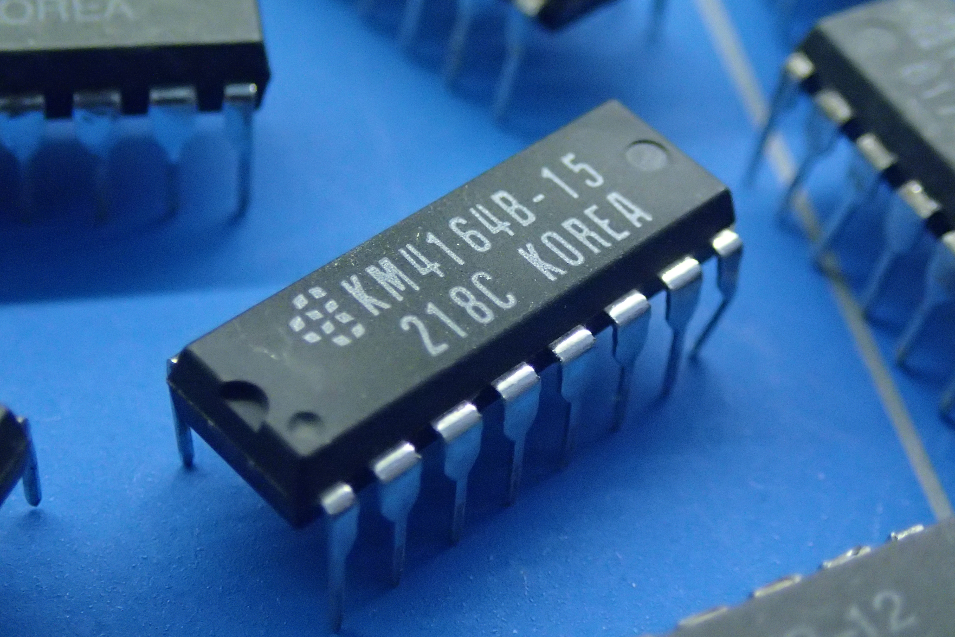
The 4164 DRAM memory chips can be found inside old 8-bit computers like Atari 800XL and Commodore 64. In this blog, I will try to explain how they work by going through the datasheet and then building a breadboard with an Arduino to look at the operation in more detail.
Looking at the datasheet of 4164 DRAM we can read in the general description that it is a dynamic ram access memory with 65536 bits. Dividing that number by 8 will give us 8192 bytes which is equivalent to 8 kilobytes. The chip is available in 3 different access speeds 100, 120 and 150 nanoseconds and it operates on 5V TTL voltage, so which means that we can safely use it with an Arduino board.
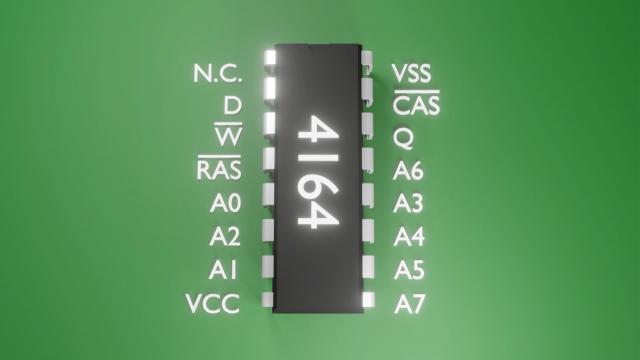
The chip has 16 pins of which 8 of them are used for addressing. Then we have pins for row and column address strobes called RAS and CAS, a write enable pin, and data in and out pins.
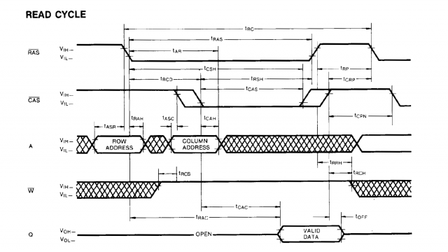
The memory inside the chip is arranged in 256 rows and 256 columns. To read one bit from a memory location, first the row address is set on the address pins and the RAS pin is brought LOW. The same is done with the column address and the CAS pin. Now the data bit can be accessed on the Data OUT (Q) pin.
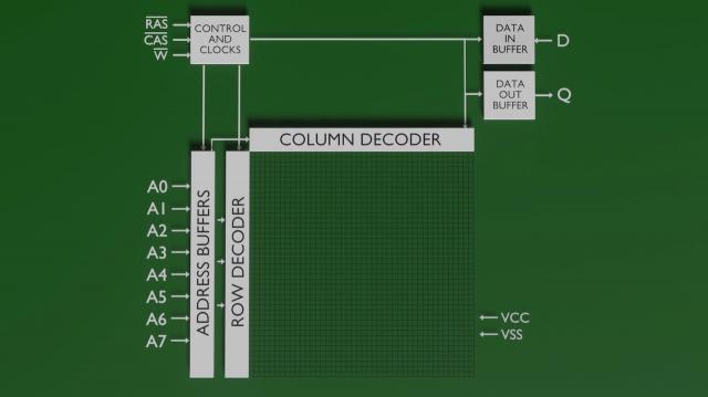
The write operation works in a similar way. The row address is set, then the write pin is brought LOW and the data bit destined to be written can be set alongside the column address. When the CAS pin is brought LOW the memory address is updated with the new value that is on the D pin.
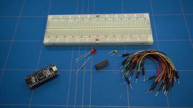
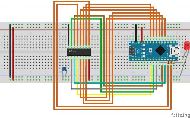
To build our DRAM tester I will be using a breadboard, Arduino Nano, 100 nF bypass capacitor, LED with 220 Ohm current limiting resistor and some jumper wires.
First we are going to insert the Arduino Nano in the breadboard, then the 4164 DRAM chip. And now the bypass capacitor. On pin 7 of the Arduino, we will add the current limiting resistor together with the LED. Note that the negative wire of the LED, the cathode is connected to the ground.
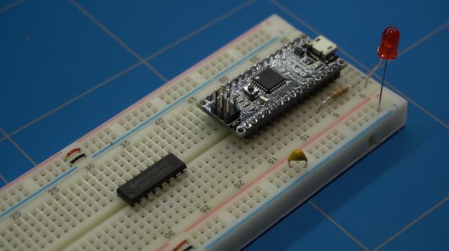
Now we can start connecting jumper wires. 5 Volts of the DRAM chip is pin 8 and ground is pin 16. We will do the same with the Arduino.
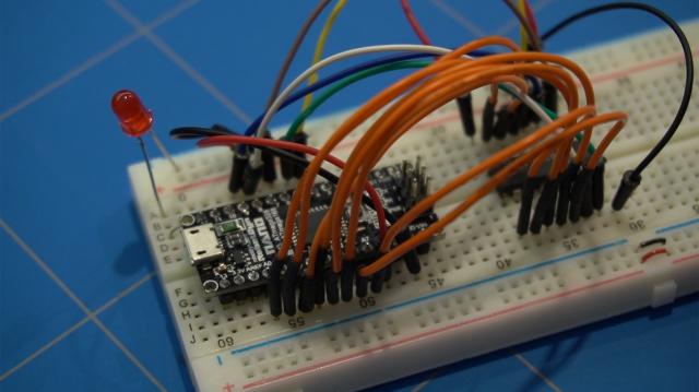
Then we will connect the RAS pin on the chip, which is pin 4 to pin 4 of the Arduino. CAS is pin number 2 and it connects to pin 5 of the Arduino. The D pin on the DRAM chip connects to pin 6 and the Q - which is the data out pin to pin 8 on the Arduino. The last of the specially designated pins on the DRAM chip is the W pin number 3 that we will connect to pin 9 on the Arduino.
To finish up quickly we will connect A0 through A7 on the DRAM chip to the equivalent A0 ... A7 pins on the Arduino. I am making a mistake here... that we will find out later.
Let's create a sketch that will write all ones to every single cell of the DRAM chip. This isn't by any means a valid test of the chip, but we are simply trying to learn how to read and write data onto it. Check the sketch below that is created with Arduino web editor or visit the Arduino editor page. Layout and schematics are also provided.
Code explanation:
The first lines of code (5-10) are just some declarations for the pins that we have connected earlier. In the setup function, we are defining what pins are input and what are output. Only the Q pin, which outputs data on the DRAM chip is defined as an input on the Arduino.
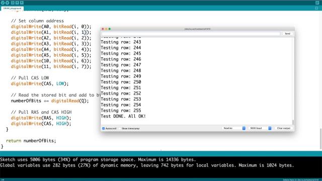
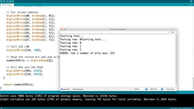
In the loop function, we are writing data to all the 256 rows and then reading it back. If the number of ones inside a row is not equal to 256 then we throw an error and stop the code. When the test is successful we blink the LED.
To understand the write function we need to pull up the timing diagram of the write cycle from the datasheet. I am not going to focus on the timing values themselves as the chip is very forgiving. Only the sequence of events matters in our case. Also because we are using an Arduino which runs at a clock speed of 16MHz we would have to do our best to exceed the minimum timing limits. As one instruction cycle is 62.5 nanoseconds and this is only achievable when we use assembler instructions and direct port register mappings, which we will not in this example.
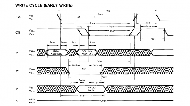
Getting back to our code and the timing diagram we can see that the write cycle starts when RAS and CAS is pulled HIGH. This is what we do first in our code using the Arduino digitalWrite() function. The next event is to set the row address, which is done by setting all the bits individually from the passed row variable. Next, we can pull the RAS pin LOW to strobe in the row address. After that, we can pull the write enable pin to LOW and set the data bit value to 1. At this point, we can continue to set the column address of the row that we are currently in. Finally, we can pull CAS LOW and right after that reset RAS and CAS to high and continue looping through the rest of the columns.
The read function is very similar to the write function. The difference is in the write signal that is now pulled HIGH during the whole cycle. For the fastest 4164 chip, valid data on the Q pin is available after 100 nanoseconds when the RAS pin is brought LOW. In the read function, we are counting the bits that were previously set in the write function and returning the sum so it can be checked.
We can now compile and upload our sketch. However after we execute it, there is an error in the match of the number of bits that were written and read back from the chip. It took me a long time to figure out what the problem was. First I thought that the Arduino was too slow, but there were other projects out there that seem to work OK with DRAM chips. The solution however was very simple.
The mistake was using pins A6 and A7 on the Arduino Nano board, which do not work. This is because these pins are true analogue pins. To quickly fix this swap A6 to D10 and A7 to D11. Below you can see the complete layout of the breadboard created with the Fritzing app
The code above already contains the fix as I didn't want to share code that does not work, but you can break it and replace pins 10 to A6 and 11 back to A7.
Now compiling and running the program shows the correct working of the chip. We can write and read back all 256 rows and columns without any errors.